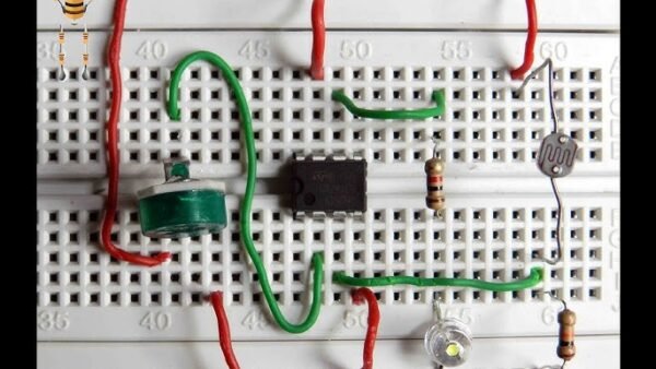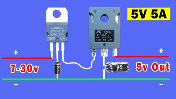
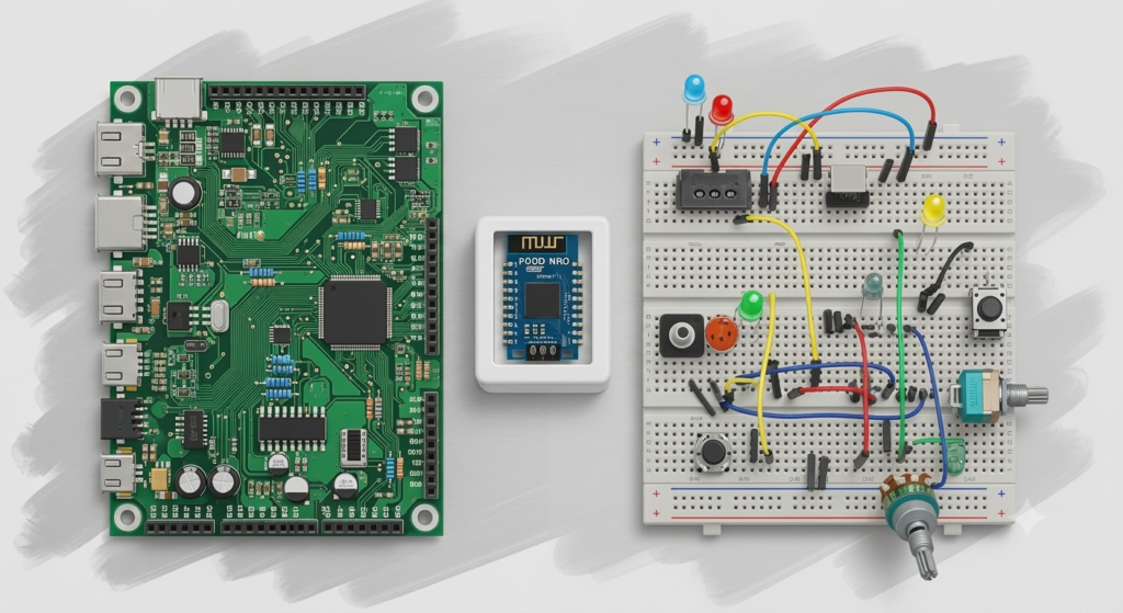
Breadboards are wonderful liars: they hide parasitic capacitance, forgive loose contacts, and fall apart in your backpack. The day you want five copies of a circuit — or one copy that survives vibration — you need a printed circuit board. Modern fabrication is astonishingly accessible: design free in KiCad, upload files, and receive five professional boards for the price of a pizza. This tutorial walks the complete workflow, from a validated schematic to unboxing, using the habits that keep first boards from becoming expensive coasters.
Step 1: Freeze a Tested Schematic
Never design a PCB around an untested idea. Build the circuit on a breadboard first, measure it, abuse it a little — and only then capture the schematic. In your CAD tool (KiCad is free and industry-grade), place symbols, wire them, and annotate. Run the Electrical Rules Check (ERC): it catches unconnected pins, outputs wired together, and missing power flags. Assign every symbol a real footprint now — the resistor is not “a resistor” but an 0805 SMD or a through-hole axial part with specific pad spacing. Choosing footprints while shopping carts are open, with parts you can actually buy, saves the most common beginner heartbreak.
Step 2: Lay Out the Board
Import the schematic into the PCB editor and placement begins — the step that separates functional boards from elegant ones. Order of operations that works: connectors at the edges first, then the largest parts, then group each IC with its support components. Keep decoupling capacitors millimeters from the power pins they serve. Route power traces wider than signal traces (0.5 mm minimum for a few hundred mA; use an online trace-width calculator for more), keep high-speed or noisy signals short and away from analog inputs, and pour a ground plane on the bottom layer — it simplifies routing, lowers noise, and gives every ground pin a short path home. For two-layer hobby boards: signals on top, ground plane beneath.
Step 3: Design Rules Check, Then Sleep on It
Run the DRC with your fab house’s capabilities loaded (typical budget rules: 6/6 mil trace/space, 0.3 mm minimum drill). Fix everything it flags — no “it will probably be fine”. Then do the human review: print the layout at 1:1 scale and set real components on the paper. Connectors that collide, mounting holes under tall parts, and text hidden beneath components all reveal themselves instantly on paper and never on screen. Check silkscreen polarity marks for every diode, LED, electrolytic and IC. Export Gerbers (the copper layers, solder mask, silkscreen, and drill files) and preview them in a Gerber viewer before uploading.
Safe Default Order Settings
| Option | Recommended Value | Why |
|---|---|---|
| Layers / material | 2 layers, 1.6 mm FR4 | Standard, rigid, cheap |
| Copper weight | 1 oz | Enough for a few amps with wide traces |
| Surface finish | HASL (or ENIG for fine SMD) | HASL is cheapest and solders easily |
| Min trace/space | Keep design ≥ 8/8 mil | Comfortably inside budget fab rules |
| Quantity | 5 (the usual minimum) | Spares are nearly free — you will lift a pad on one |
Step 4: Fabricate, Assemble, Test
Upload the Gerber zip to a fab (JLCPCB, PCBWay, OSH Park), choose 1.6 mm FR4 with 1 oz copper, and pick your color. Two weeks later, assemble with tweezers and a fine-tip iron: lowest parts first (resistors, diodes), ICs next, tall parts and connectors last. Then test in stages: continuity-check power rails for shorts before applying power, power up with a current-limited supply, verify the 5 V rail, then feed a signal. A short found with a multimeter costs nothing; the same short found by smoke costs a board.
Tools and Materials Checklist
- KiCad (free) or EasyEDA installed
- A validated, breadboard-tested schematic
- Datasheets for every component (footprint verification)
- Fab-house design rules file for the DRC
- Fine soldering iron (0.5–1 mm tip), tweezers, flux, wick
- Multimeter with continuity mode; current-limited supply if available
Prototype Before You Commit
Even before the breadboard, sanity-check the core loop — battery, resistors, LEDs, switches — in our Circuit Simulator. Confirming currents and behavior in simulation, then on a breadboard, then on paper at 1:1 scale means the manufactured board is the fourth time you have built the circuit — and fourth versions rarely fail.
Troubleshooting First Boards
- Footprint mismatch: the classic — measure one real part against the 1:1 paper print before ordering.
- Board dead, hot spot found by finger: a solder bridge; flux and wick, then retest rails.
- Works on bench, flaky in enclosure: missing mounting holes or connectors flexing — add mechanical support in rev 2.
- Noisy analog readings: ground plane split by careless routing; keep a solid return path under analog signals next revision.
Safety Notes
- Solder with ventilation or a fume extractor; wash hands after handling solder and boards.
- Eye protection when cutting leads — clipped ends fly surprisingly far.
- Keep mains-voltage designs off hobby PCBs until you understand creepage and clearance distances; low-voltage projects first.
Conclusion
Schematic → ERC → footprints → layout → DRC → paper review → Gerbers → fab → staged assembly: an unglamorous checklist that turns ideas into hardware you can hold, sell, and trust. Your first board will have a mistake — everyone’s does — and revision two is where the satisfaction lives. Order the boards; you are a PCB designer now.